


ANSYS PathFinder helps you plan, verify and sign-off IP and full-chip SoC designs for integrity and robustness against electrostatic discharge (ESD). The analysis is performed at the layout and circuit levels to help you identify and isolate design issues that can cause chip or IP failure from charged-device model (CDM), human body model (HBM) or other ESD events.
Using layout and circuit-level analysis you can identify and isolate design issues that can cause chip or IP failure due to charged-device model (CDM), human body model (HBM) or other ESD events.
More About ANSYS PathFinder
- PathFinder is certified by a number of foundries as an ESD sign-off solution, giving you the assurance that the interconnect parasitic extraction, HBM/CDM ESD simulation and current-density checks on ESD discharge paths are accurate by foundry standards.
- PathFinder offers layout-based analysis and a GUI for detecting layout issues that could lead to ESD events.
Capabilities of ANSYS PathFinder
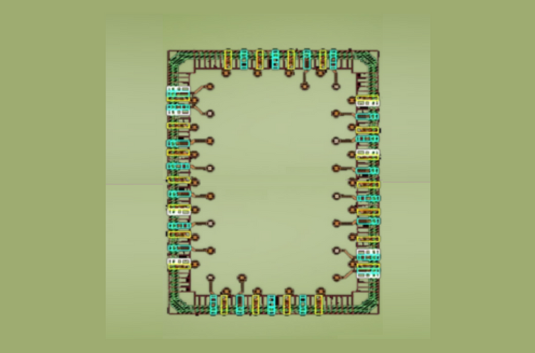
Electrostatic discharge integrity: IP to SoC
PathFinder provides you with comprehensive coverage of on-chip ESD events, which is a requirement for most chip designs.
PathFinder’s integrated data modeling, extraction and simulation engine offer you an end-to end-solution for ESD verification.
RedHawk offers you the capacity and performance to simulate designs having over 1 billion instances using advanced Distributed Machine Processing (DMP) techniques.
Increasing current densities in advanced technologies lead to more ESD issues. PathFinder provides accurate ESD analysis prior to sign-off to ensure first-time silicon success.
With distributed computing, PathFinder can simultaneously handle hundreds of domains in one analysis for faster turnaround.
PathFinder offers you the coverage, accuracy, capacity and performance to address ESD issues from standard cell to SoC levels of design.